Q&A: Katayun Barmak
Philips Electronics Professor in Applied Mathematics and Applied Physics
 Barmak stands in the newly constructed Electron Microscopy (EM) Laboratory located on the first floor of Havemeyer Hall.
(Photo by Jeffrey Schifman)
Katayun Barmak is aiming to define structure-property relationships of metals in engineered high-tech systems like data storage, integrated circuits, and advanced permanent magnets. As an experimental materials scientist, Barmak spends the majority of her time in the lab, peering into electron microscopes to study the very minute, nanometric-scale structure of materials, with the hope of finding the link between their structure— for example, the three-dimensional arrangement of the nanocrystals—and their properties, whether it’s electrical conductivity or magnetic hardness.
“I’m very interested in basic studies that explore the relations between how you make a material, what its structure is, and then, how it behaves. Is it a good or poor conductor of electricity, and so on,” explains Barmak, the Philips Electronics Professor in Applied Mathematics and Applied Physics. “I find it very exciting because I like to work on that edge of science where I can see the application. I want to know that the science will be used; I’m interested in the underlying science of the material that goes into building even just a small part of an engineered system.”
Before joining Columbia Engineering in 2011, Barmak was on the faculty at Carnegie Mellon University, where she rose to full professor in just three years. She was one of the first materials scientists ever to successfully map the crystallographic orientation of polycrystalline structures on the nanoscale for statistically significant populations. An exciting research feat at the time—four years ago—when high throughput crystal orientation mapping methods at the nanoscale were not available. But now the technique is readily available, making it possible, for example, to see how metallic elements like copper can be tailored to be even better nanoscale electrical conductors.
Shortly after the fourth of July holiday, Barmak talked to Columbia Engineering magazine about her ongoing work in metals on the nanoscale, setting up the School’s new electron microscopy lab, and her previous life in the performing arts.
Q: How did you get your start in metallurgy?
A: I went to Cambridge as an undergraduate and started in natural sciences to give me some flexibility in the choice of classes. I had to pick a last class. I had only been in England for two years. To me, English was still a second language, although I spoke it very well, so I was trying to avoid any classes where essay assignments were involved. Ironically, all I do now is write, and I was trying to avoid writing. There was only one class without essays and it was Crystals. We started to do a lot of visible light microscopy of crystals, and the images were beautiful. What you can see in the microscope, those images, just grabbed me. I spent a lot of my time collecting images, analyzing images, extracting information from images. And, I love art. I love the visual arts, the performing arts, and painting. For me, the images were beautiful, appealing in their own right; but also what kept my interest was the information content extracted from those images. The images led to the science.
Q: The performing arts were actually a big part of your life at one point.
A: I wanted to be a ballet dancer. I started at age 8. In the end, I did ballet on and off for 25 years. I danced in graduate school and afterwards. I danced with chamber ballet companies. In a dance class, your mind is completely engaged in trying to learn the steps, keep to the music, keep to the time. It’s physically and mentally so fully engrossing that you come out of class exhausted but also refreshed. I miss it terribly. It was the best thing. So initially I wanted to become a ballet dancer. Now, I look back on the insanity of that. I grew up in Iran, but at the time of rapid growth and modernization. The country had a ballet company that I could join. And we had dancers and teachers from all over the world. It was just this phenomenal pocket of time where we thought we were dancing on the world stage . . . but then my parents thought this was absolutely not the career for me. [Laughs] And in retrospect, it was a very lucky thing I didn’t do it.
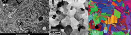
From left to right: Bright-field transmission electron micrograph of stained mouse lung tissue; bright-field transmission electron micrograph of an aluminum film; crystal orientation map of a copper film.
(Images courtesy of Katayun Barmak)
Q: You’re currently doing a lot of research on the nanoscale. What is the materials science field like now?
A: It’s an exciting time. It’s exciting because now our instrumentation and our computing power are beginning to match our desires. The computing power that wraps around every instrument is making things so much better and enabling new science. In materials, for me, it’s a very exciting time because we do not yet have the full predictive theories in materials that will allow us to design a material for an engineered system in a computer, then go and make it and have it behave the way we wanted. But we’re getting there. Some of what [Associate Professor] Chris Marianetti and others do—computing materials from the principles of quantum mechanics—and some of the materials and properties predicted we’re now able to measure and verify. We’re beginning to get glimpses of what we can do.
Q: What is the end goal?
A: To find new or better materials—there’s always newer and better defined by some figure of merit. Hopefully, the new is better. [Laughs]
Q: This academic year, faculty, students, and researchers across Columbia will have access to the School’s new Electron Microscopy (EM) Lab in Havemeyer. This is significant.
A: It has been exciting (and, at times, exasperating) constructing this new central facility for not only our faculty and students, but for other Columbia members and alumni. I am looking forward to the creativity we’re going to get out of its use, the world-class science that will come out of it from researchers using the instrument and who are doing exciting work here. I think we’ll be blown away!