Aron Pinczuk + Shalom Wind: Artificial Graphene—Better than the Real Thing?
Artificial Graphene—Better than the Real Thing?
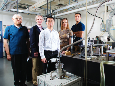
From right to left: The Artificial Graphene team—Diego Scarabelli, Yuliya Kuznetsova, Sheng Wang, Shalom Wind, and Aron Pinczuk.
(Photos by Jeffrey Schifman)
Working at the cutting edge of physics at the nanoscale, Aron Pinczuk and Shalom Wind are developing new ways to access quantum mechanical phenomena by manipulating matter at nanoscale dimensions. One of the areas they are especially interested in is artificial graphene, a material that is now attracting more and more attention because researchers believe it will have more versatile properties than the real thing.
“This is a rapidly expanding area of research,” says Wind, adjunct professor and senior research scientist in the Department of Applied Physics and Applied Mathematics. “We are uncovering new phenomena that couldn’t be accessed before. As we explore novel device concepts by engineering the artificial graphene in different ways, we can unlock the potential to expand frontiers in quantum mechanics, with potential applications in advanced optoelectronics and data processing.”
Graphene has highly unusual electronic properties: its electrons can travel great distances before they are scattered, making the material an outstanding conductor. In addition, the way atoms are arranged in graphene causes them to behave as if they are relativistic particles that have zero mass and can move close to the speed of light, fueling hopes for hyperfast electronics and more.
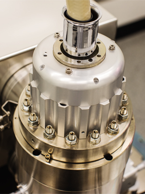
The Nanobeam nB4 electron beam lithography system, shown here, uses a finely focused beam of electrons to “write” nanoscale patterns that define the artificial graphene lattice. The nB4 is one of the critical tools within the Columbia Nano Initiative that enable leading-edge nanoscience research.
“These properties are very exciting because they can lead to the observation of exotic quantum mechanical states,” says Pinczuk, professor of applied physics and physics, who uses optical methods to examine nanostructures. “But accessing these states in natural graphene is challenging, because handling single atomic layers entails extremely complex operations.”
While researchers have been trying to create artificial graphene in semiconductors, until now they have been unable to reach the small dimensions required to create an interconnected electronic lattice. The Columbia Engineering team’s latest breakthrough has been to recreate, for the first time, the electronic structure of graphene in an engineered semiconductor. Using the tools of conventional chip technology, they made quantum dots—instead of carbon atoms—in a gallium arsenide-based semiconductor and organized them in a honeycomb lattice, mimicking the graphene crystal structure. Once the quantum dots were placed close enough to each other that they could share electrons, they displayed the electronic signature of graphene.
This artificial graphene has several advantages over natural graphene; for instance, researchers can design variations into the honeycomb lattice to modulate electronic behavior. And because the spacing between the quantum dots is much larger than the interatomic spacing in natural graphene, researchers will be able to observe even more surprising quantum phenomena with the application of a magnetic field.
“It will be easier to make observations with the artificial graphene we’ve developed,” Pinczuk notes. “Potential applications include new types of electronic switches, novel photodetectors and transistors with superior properties, and even perhaps new ways of storing information based on novel quantum mechanical states. And we’ve created a new materials base to explore intriguing quantum physics.”
He and Wind are now working on the next generation of artificial graphene devices, which will have more closely spaced lattices, making it easier to observe electronic states. They will use the devices for experiments at high magnetic fields as well as transport experiments, where they measure current through the artificial graphene lattice.
“This is an exciting time for those of us working in nanoscience,” Wind adds. “As our ability to structure matter at increasingly small dimensions continues to improve, we’ll be able to observe newer and more exotic phenomena and create materials, like artificial graphene, that we’ve only been able to dream about.”